
NOTE: As previously stated, NVIDIA's board partners will be releasing there own card designs so the following should be viewed with this in mind as it may not follow what is found on retail versions.

The cooling on the GTX650Ti BOOST is a reference design heatsink and thus comprises of an enclosed unit which sucks air in from the fan and then pushes the air over the heatsink with the resulting hot air exhausted out of the vented IO plate at the rear of the card.

The actual PCB of the GTX650Ti has a very small PCB, measuring just 173mm in length compared to the GPU's overall length of 240mm. With small form factor PC's popularity on the rise, the GTX650Ti Boost will prove to be popular because of this small footprint.

The GTX650Ti Boost has a 4+1 power phase design which is increased over the 3 phases of power afforded to the GPU in the stock reference GTX650Ti, most likely due to the additional overclocking/power requirements of this new design.
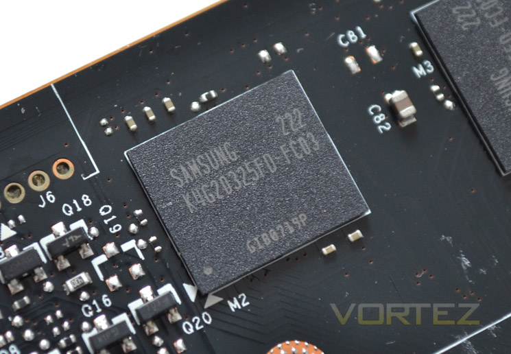
The GDDR5 memory hails from Samsung and is an 8x256MB (2GB) design (4 on the back, four on the front). Rated to 6000MHz (effective) the product code of K4G20325FD tells us that the VRam has a Vdd/Vddq(V) of 1.455 to 1.545. How this will effect our overclocking results remains to be seen but with it being so highly clocked, we doubt it can be pushed much further if previous results are anything to go by which is no bad thing as this allows us to concentrate on overclocking the core!
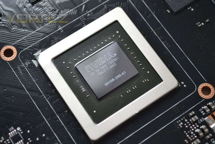
The GK106 Core is built on the same 28nm manufacturing process as the rest of the Kepler family. Equipped with 768 CUDA cores and an improved 192 bit memory interface the GTX650Ti Boost along with overclocking now enabled (GPU Boost) should make this little card a little powerhouse.
Let's take a look at today's test setup and methodology...
Cooling
The cooling on the GTX650Ti BOOST is a reference design heatsink and thus comprises of an enclosed unit which sucks air in from the fan and then pushes the air over the heatsink with the resulting hot air exhausted out of the vented IO plate at the rear of the card.
Naked
The actual PCB of the GTX650Ti has a very small PCB, measuring just 173mm in length compared to the GPU's overall length of 240mm. With small form factor PC's popularity on the rise, the GTX650Ti Boost will prove to be popular because of this small footprint.
VRM
The GTX650Ti Boost has a 4+1 power phase design which is increased over the 3 phases of power afforded to the GPU in the stock reference GTX650Ti, most likely due to the additional overclocking/power requirements of this new design.
Memory
The GDDR5 memory hails from Samsung and is an 8x256MB (2GB) design (4 on the back, four on the front). Rated to 6000MHz (effective) the product code of K4G20325FD tells us that the VRam has a Vdd/Vddq(V) of 1.455 to 1.545. How this will effect our overclocking results remains to be seen but with it being so highly clocked, we doubt it can be pushed much further if previous results are anything to go by which is no bad thing as this allows us to concentrate on overclocking the core!
GK106 Core
The GK106 Core is built on the same 28nm manufacturing process as the rest of the Kepler family. Equipped with 768 CUDA cores and an improved 192 bit memory interface the GTX650Ti Boost along with overclocking now enabled (GPU Boost) should make this little card a little powerhouse.
Let's take a look at today's test setup and methodology...


